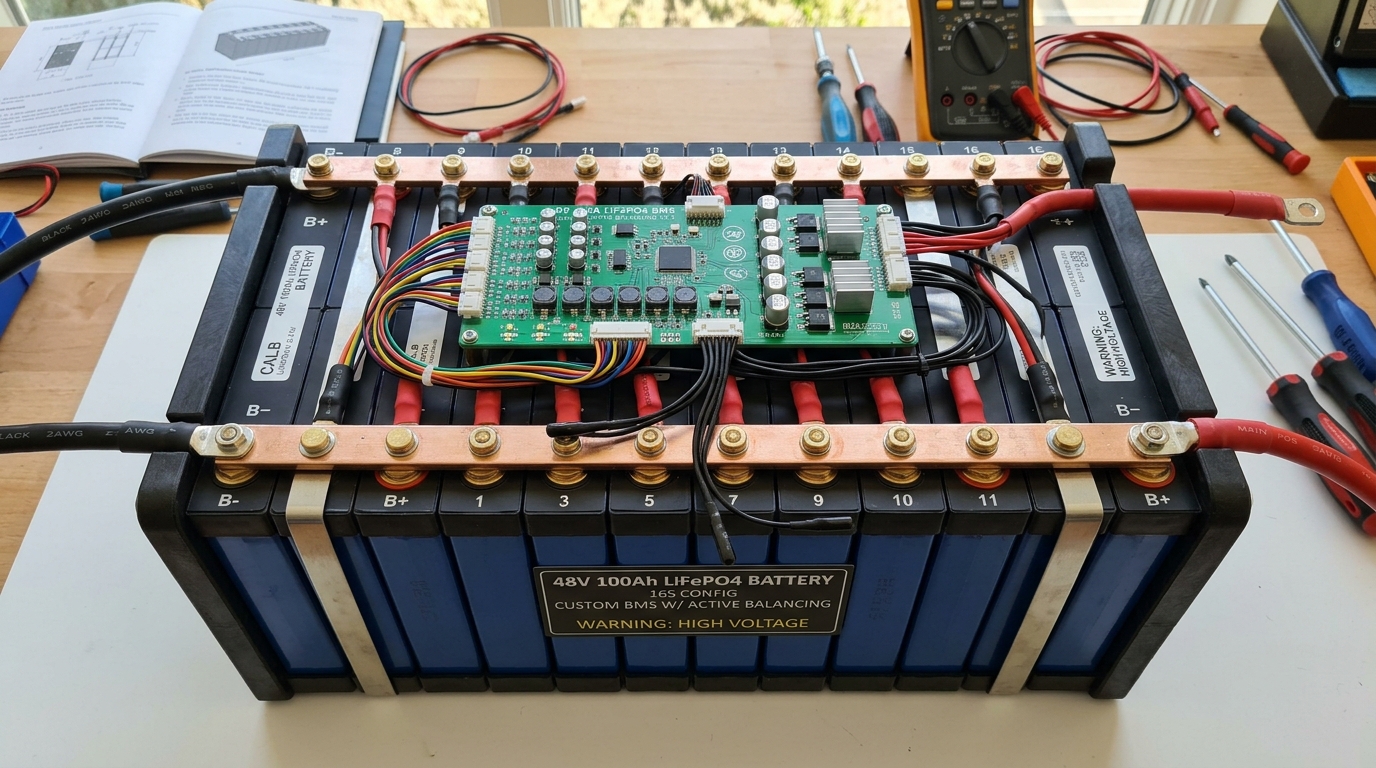
Gallium Nitride (GaN) Power Electronics: Designing High-Efficiency 140W USB-C PD 3.1 Supplies
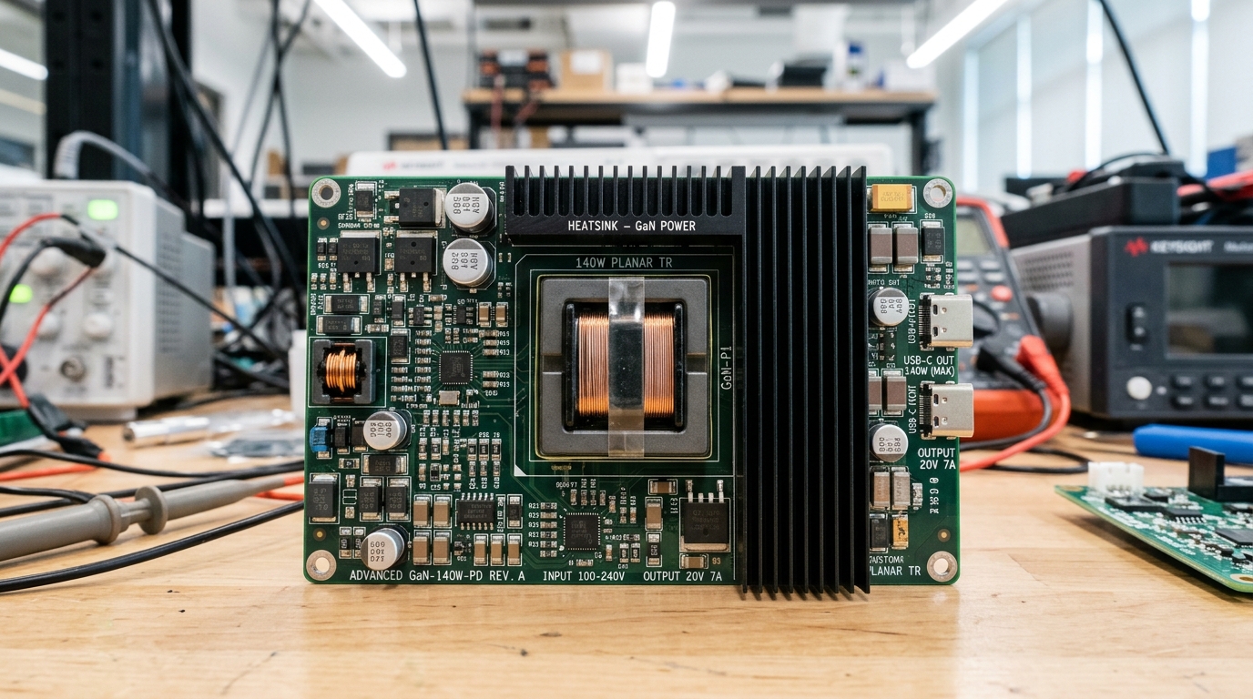
Table of Contents
“Gallium Nitride (GaN) high-electron-mobility transistors (HEMTs) are revolutionizing power supply engineering. With dramatically lower gate charge (Qg) and near-zero reverse recovery charge (Qrr), GaN devices enable switching frequencies from 500 kHz to over 1 MHz. This allows engineers to shrink magnetics and achieve ultra-high power densities exceeding 20 W/in³.”
1. Active Clamp Flyback (ACF) Topology vs. Traditional Flyback
Traditional flyback converters dissipate primary leakage inductance energy as heat through RCD snubber networks, limiting peak efficiency to roughly 88%. By adopting an Active Clamp Flyback (ACF) topology, leakage energy is recycled into the input filter capacitor, enabling Zero-Voltage Switching (ZVS) across the primary GaN FETs.
Key Engineering Takeaways
- Zero-Voltage Switching (ZVS) eliminates primary turn-on switching losses
- Recycles transformer leakage inductance energy directly to the output stage
- Enables 94%+ full-load power conversion efficiency in compact form factors
2. Critical PCB Layout Rules for High-Frequency GaN Gate Drives
Because GaN HEMT gate threshold voltages (Vgs(th)) are low (~1.7V) and absolute maximum gate voltage ratings are restricted (~6.0V), even sub-nanohenry parasitic gate loop inductance can trigger destructive voltage overshoot or false turn-on during high dV/dt switching (>100 V/ns).
// GaN Gate Driver PCB Loop Optimization Rules
1. Place gate driver IC directly adjacent to GaN FET (< 3 mm loop distance).
2. Minimize Gate-Source loop area using a dedicated underlying GND return plane.
3. Use an anti-parallel Schottky diode across gate resistor for ultra-fast turn-off.
4. Implement a dedicated Kelvin Source connection to decouple power di/dt from the gate loop.
3. Planar Transformer Integration & Thermal Spreading
Traditional wire-wound transformers suffer from severe AC copper losses at 500 kHz due to skin and proximity effects. Replacing wire windings with multi-layer PCB copper tracks inside a planar E-core provides predictable leakage inductance, excellent thermal conduction to the PCB copper, and a ultra-low vertical profile.
Summary & Engineering Verdict
Combining GaN power HEMTs with planar transformers and Active Clamp Flyback controllers allows hardware teams to manufacture ultra-compact 140W USB-C power adapters operating at over 94% efficiency.
Frequently Asked Questions
Why is a dedicated Kelvin source connection critical for GaN FETs?
A Kelvin source connection isolates the high-current power ground return from the low-power gate driver return, preventing high power di/dt voltage spikes across parasitic source inductance from corrupting the gate signal.
How do planar transformers compare to traditional wire-wound transformers?
Planar transformers use PCB copper layers instead of wire coils. This provides exact repeatability of parasitics, superior heat dissipation into the PCB ground planes, and significantly reduced height.
Power Electronics & High-Efficiency BMS Engineering
CircuitBEES designs high-density GaN/SiC power converters, custom planar magnetics, and battery management systems up to 100kW.

CircuitBEES Engineering Team
Verified Engineering TeamThe CircuitBEES engineering group brings together senior PCB layout artists, mechatronics designers, and embedded systems developers. By publishing our hands-on findings from high-speed memory tuning to deep mechatronic systems—such as our landmark countertop appliance, India's first fully automatic roti maker—we aim to raise the standard for hardware documentation.
Share this guide with your team
Help other hardware and embedded engineers optimize their designs.