
2.4GHz & 5GHz RF PCB Design: Impedance Matching, Coplanar Waveguides & Antenna Integration
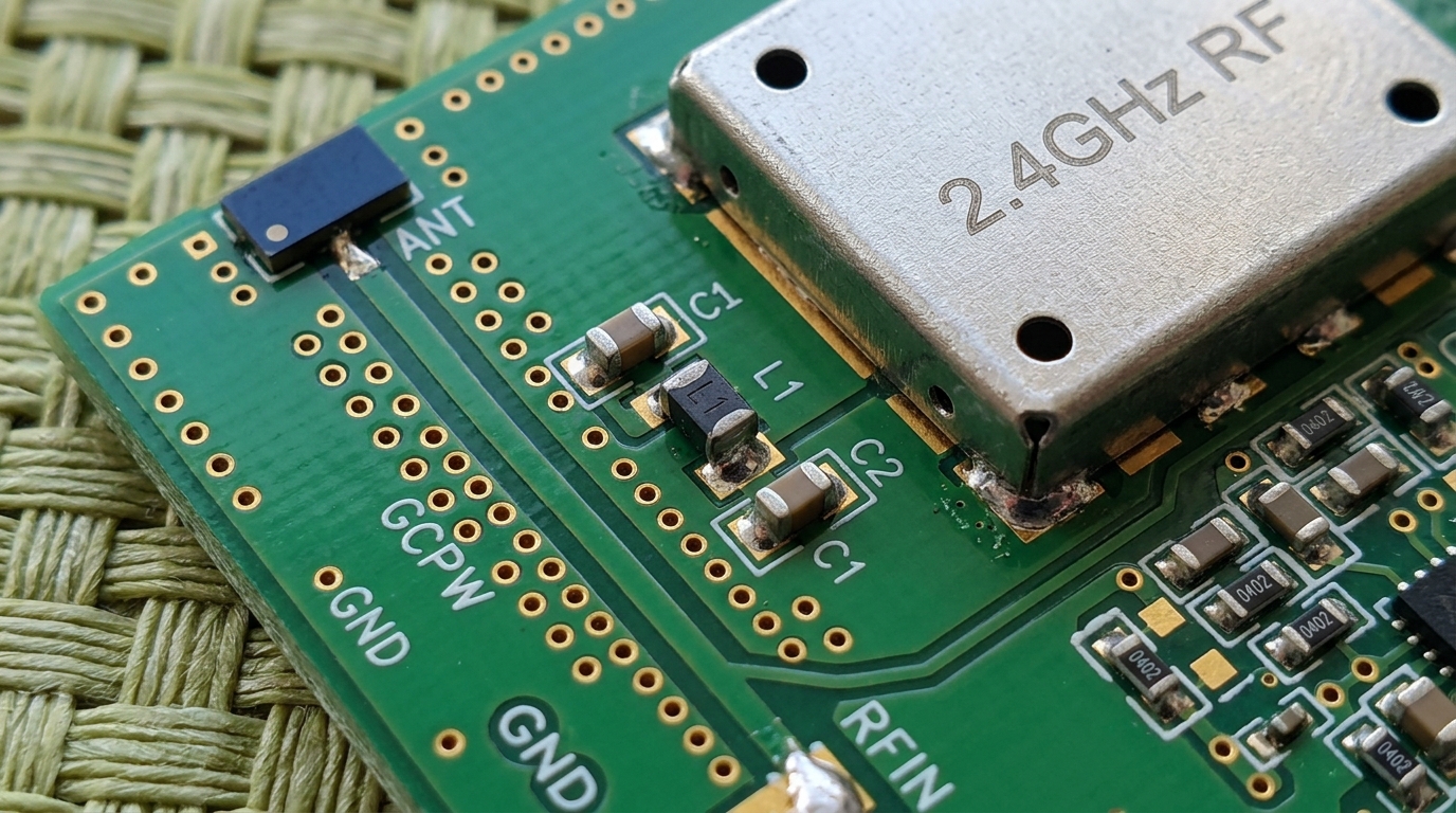
Table of Contents
“Designing high-performance Wi-Fi 6, Bluetooth Low Energy (BLE), and LoRa wireless hardware requires strict adherence to 50Ω RF transmission line rules. A small mismatch in trace geometry or ground clearance will reflect RF power back into the transmitter, reducing wireless range and failing FCC/CE radiation testing.”
1. Grounded Coplanar Waveguide (GCPW) Geometry
Grounded Coplanar Waveguide (GCPW) routing features a central signal trace flanked by ground planes on the same layer, with a continuous ground plane underneath. Flanking ground copper with tightly spaced stitching vias provides excellent isolation against crosstalk from nearby digital lines.
Key Engineering Takeaways
- Trace Width & Gap: Calculate exact 50Ω geometry using dielectric constant (Er) and substrate height
- Via Stitching: Place ground stitching vias along the RF channel at less than λ/10 spacing (1.2 mm for 2.4GHz)
- Keepout Zone: Maintain complete copper-free clearance under ceramic chip and PCB trace antennas
2. Tuning Pi-Matching Networks with Smith Charts
A three-element Pi-network (Shunt-Series-Shunt) placed between the RF transceiver and the antenna allows engineers to match the complex antenna impedance to 50Ω. Using a Vector Network Analyzer (VNA), component values are plotted on a Smith Chart to eliminate reactive inductive or capacitive mismatches.
// 2.4GHz Pi-Network Matching Example
[RF Transceiver] ---> [C1: Shunt 1.2pF] ---> [L1: Series 3.3nH] ---> [C2: Shunt 0.5pF] ---> [Antenna]
Measured VSWR before tuning: 2.8:1  (35% power reflected)
Measured VSWR after Pi-tuning: 1.15:1 (< 0.5% power reflected)
3. Ceramic Chip Antennas vs. Inverted-F PCB Trace Antennas
Meandered Inverted-F Antennas (MIFA) printed directly onto the PCB cost zero extra BOM, but require significant board real estate (~15mm x 6mm). Ceramic chip antennas save space (~3.2mm x 1.6mm), but require strict ground keepout areas across all PCB layers underneath the antenna body.
Summary & Engineering Verdict
Controlled 50Ω coplanar waveguide geometry, ground stitching vias, and VNA-calibrated Pi-network tuning guarantee maximum wireless range and effortless RF compliance certification.
Frequently Asked Questions
Why is a ground keepout zone necessary under a ceramic chip antenna?
Metal copper planes under or directly adjacent to an antenna attenuate the electromagnetic field, lowering radiation efficiency and shifting the resonant frequency away from the intended band.
What is VSWR and why does it matter in RF design?
VSWR (Voltage Standing Wave Ratio) measures how efficiently RF power is transmitted to the antenna. A VSWR near 1.0:1 means almost all power is radiated, while higher values mean power is reflected back into the transmitter.
RF & High-Frequency Wireless Hardware Engineering
CircuitBEES designs custom 2.4GHz, 5GHz, LoRa, and cellular wireless PCBs with complete antenna simulation and VNA impedance tuning.

CircuitBEES Engineering Team
Verified Engineering TeamThe CircuitBEES engineering group brings together senior PCB layout artists, mechatronics designers, and embedded systems developers. By publishing our hands-on findings from high-speed memory tuning to deep mechatronic systems—such as our landmark countertop appliance, India's first fully automatic roti maker—we aim to raise the standard for hardware documentation.
Share this guide with your team
Help other hardware and embedded engineers optimize their designs.